
ERC Nano-Harvest
Involved People
Principal Investigator:
Maria Tchernycheva
PhDs :
4 PhD thesis were defended during the project :
Martina Morassi
Lu Lu
Omar Saket
Camille Barbier
Postdocs :
Chalermchai Himwas
Lorenzo Mancini
Junkang Wang
Permanent researchers and engineers:
Fabrice Oehler
Jean-Christophe Harmand
Noëlle Gogneau
Nathalie Isac
Fabien Bayle
Project summary
NanoHarvest project explores novel solutions for flexible solar cells, piezoelectric converters and light emitting diodes enabled by semiconductor nanowires. The main building block is the free-standing membrane containing polymer-embedded nanowires which can be stacked in a multi-functional device and applied to almost any supporting material such as plastic, metal foil or even fabrics. The crucial ingredient and also the common basis for PV, piezo and LED devices are the advanced nanowire heterostructures: we develop nanowires with new control-by-design functionalities by engineering their structure at the nanoscale. The main focus of NanoHarvest is on the III-nitride semiconductors, which are characterized by a strong piezoelectric response and have also demonstrated their ability for efficient photon emission as well as harvesting in the blue and green parts of the visible spectrum. Our strategy is to address the physical mechanisms governing the energy conversion from the single NW level up to the macroscopic device level. The deep understanding gained at the nanoscale guides the optimization of the device architecture, of the material growth and of the fabrication process. The transfer procedure of the ordered nanowire arrays onto flexible substrates enables lightweight flexible devices with ultimate performance, which can serve as light emitters or energy harvesters for nomad applications.
Project highlights
1. Flexible Light Emitting Diodes Based on Vertical Nitride Nanowires
Flexible light emitting diodes (LEDs) are today a topic of intense research, motivated by their interesting applications such as rollable displays or lightning. Today organic LEDs are the key technology for these applications. However, OLEDs still face the issue of a poor time stability and low luminance in the blue spectral range. The technology providing the best performance in terms of luminance and EQE in the blue spectral range relies on nitride semiconductors. Thanks to this promising performance of nanowire LEDs, polymer-embedded nanowires offer an elegant solution to create a light emitter, which combines the high brightness and the long lifetime of inorganic semiconductor materials with the high flexibility of polymers.
- Flexible bi-color light emitting diodes based on nitride nanowires
We demonstrated large area (several square cm) fully flexible blue and green LEDs based on core/shell InGaN/GaN nanowires grown by MOCVD. Nanowires were embedded into PDMS layers and mechanically lifted from their growth substrate. Conductive transparent electrodes to these composite membranes were realized using silver nanowire networks. The LEDs exhibited rectifying behavior with a low reverse leakage and a light-up voltage around 3 V. The devices showed bright emission with no performance degradation neither under outward or inward bending down to 3 mm curvature radius nor in time for more than one month storage in ambient conditions without any protecting encapsulation. Fully transparent flexible LEDs with a high optical transmittance (60% at λ=530 nm) were also realized. Finally, we demonstrated the integration of green and blue LED membranes into a two-layer bi-color nanowire-based flexible LED. The two layers containing InGaN/GaN nanowires with different In contents could be either separately driven to generate green or blue light or simultaneously biased to generate a broad electroluminescence spectrum.

[Dai15] Xing Dai, Agnes Messanvi, Hezhi Zhang, Christophe Durand, Joël Eymery, Catherine Bougerol, François H Julien, Maria Tchernycheva « Flexible Light-Emitting Diodes Based on Vertical Nitride Nanowires» Nano Letters 15 (10), 6958-6964 (2015).
[Gua17] Nan Guan, Xing Dai, Andrey V Babichev, François H Julien, Maria Tchernycheva “Flexible inorganic light emitting diodes based on semiconductor nanowires” Minireview in Chemical Science 8, 7904-7911 (2017) doi 10.1039/C7SC02573D
[Gua20] Nan Guan, Nuño Amador-Mendez, Arup Kunti, Andrey Babichev, Subrata Das, Akanksha Kapoor, Noëlle Gogneau, Joël Eymery, François Henri Julien, Christophe Durand, Maria Tchernycheva, “Heat dissipation in flexible nitride nanowire light-emitting diodes” Nanomaterials 10 (11), 2271 (2020)
[Koch21] Kochetkov, FM, Neplokh, V, Mastalieva, VA, Mukhangali, S, Vorob'ev, AA, Uvarov, AV, Komissarenko, FE, Mitin, DM, Kapoor, A, Eymery, J, Amador-Mendez, N, Durand, C, Krasnikov, D, Nasibulin, AG, Tchernycheva, M, Mukhin, IS, « Stretchable Transparent Light-Emitting Diodes Based on InGaN/GaN Quantum Well Microwires and Carbon Nanotube Films” NANOMATERIALS 11 (6), 1503 (2021) doi 10.3390/nano11061503)
- Flexible white light emitting diodes based on nitride nanowires and nanophosphors
We have demonstrated a flexible white phosphor-converted LED based on p-n junction core/shell nitride nanowires. GaN nanowires containing 7 radial In0.2Ga0.8N/GaN quantum wells were grown by metal-organic chemical vapor deposition on a sapphire substrate by a catalyst-free approach. To fabricate the flexible LED, the nanowires are embedded into a phosphor-doped polymer matrix, peeled off from the growth substrate and contacted using flexible and transparent silver nanowire mesh. The electroluminescence of a flexible device presents a cool-white color with a spectral distribution covering a broad spectral range from 400 to 700 nm. Mechanical bending stress down to a curvature radius of 5 mm does not yield any degradation of the LED performance. The maximal measured external quantum efficiency (EQE) of the white LED is 9.3% and the wall plug efficiency is 2.4%.

[Gua16] Nan Guan, Xing Dai, Agnes Messanvi, Hezhi Zhang, Jianchang Yan, E. Gautier, Catherine Bougerol, François H. Julien, Christophe Durand, Joël Eymery, and Maria Tchernycheva, Flexible White Light Emitting Diodes Based on Nitride Nanowires and Nanophosphors, ACS Photonics 3 (4), 597-603 (2016).
[Gua19] Nan Guan, Nuño Amador-Mendez, Junkang Wang, Subrata Das, Akanksha Kapoor, François H Julien, Noëlle Gogneau, Martin Foldyna, Sudipta Som, Joël Eymery, Christophe Durand and Maria Tchernycheva « Colour optimization of phosphor-converted flexible nitride nanowire white light emitting diodes » J. Phys.: Photonics 1 (2019) 035003 10.1088/2515-7647/ab2c84
2. Nanoscale analyses of nanowire LED properties
- Green m-plane InGaN/GaN nanowire LEDs
High EQE green emission is an open challenge for the LED technology. We demonstrated green emission from InGaN/GaN core/shell nanowires using low temperature MOCVD growth of the radial quantum wells. This demonstrates the possibility to produce green emitters with core-shell wire LEDs elaborated by industrially-relevant MOVPE technique.

[Kap18] Akanksha Kapoor, Nan Guan, Martin Vallo, Agnès Messanvi, Lorenzo Mancini, Eric Gautier, Catherine Bougerol, Bruno Gayral, François H Julien, François Vurpillot, Lorenzo Rigutti, Maria Tchernycheva, Joel Eymery, Christophe Durand “Green electroluminescence from radial m-plane InGaN quantum wells grown on GaN wire sidewalls by MOVPE” ACS Photonics 2018, 5 (11), pp 4330–4337; 10.1021/acsphotonics.8b00520
- Color control of nanowire InGaN/GaN light emitting diodes by post-growth treatment
The complexity of the three-dimensional active region of nanowire (NW) LEDs makes the growth control very challenging. It has been observed that in NWs with intrinsic compositional inhomogeneities the electro-luminescence (EL) depends on the contact layout. This dependence of the EL on the contact morphology opens the way to control the LED emission color at the device processing stage. Indeed, if the compositional variation cannot be avoided at the growth stage, the electrical injection in the unwanted regions can be inhibited by a dedicated post-growth treatment.
We have shown that for NW LEDs coming from the same growth run the EL color can be controlled by the contacting procedure. In particular, the pure blue emission without a spectral shift with injected current was achieved with NWs initially presenting regions of different InGaN composition. This was realized by locally reducing the conductivity of the p-doped GaN shell using fluorine plasma treatment to inhibit the electrical injection in the In-rich region of the QW. Modification of the contact layout to selectively contact the lateral m-plane facets and a post-growth CHF3 plasma treatment allowed to suppress the unwanted green contribution at medium and high injection while increasing the EL intensity in the blue spectral range. ICP etching of the In-rich region allowed to suppress the green emission for all injection currents, however the intensity loss in the blue spectral range due to ICP-induced damage was observed. The selective contacting of the m-plane and the plasma treatment of the NW top appear as a promising solution for controlling the color of core/shell NW LED with inhomogeneous internal composition.

[Zha15] Hezhi Zhang, Gwénolé Jacopin, Vladimir Neplokh, Ludovic Largeau, François H. Julien, Olga Kryliouk, Maria Tchernycheva « Color control of nanowire InGaN/GaN light emitting diodes by post-growth treatment» Nanotechnology, 26 465203A (2015).
[Zha21] Hezhi Zhang, Valerio Piazza, Vladimir Neplokh, Nan Guan, Fabien Bayle, Stephane Collin, Andrey Babichev, Francois H Julien, Maria Tchernycheva, “Correlated optical and electrical analyses of inhomogeneous core/shell InGaN/GaN nanowire light emitting diodes”, Nanotechnology 32, 105202 (2021) doi 10.1088/1361-6528/abc70e
- Electron Beam Induced Current Microscopy and Cathodoluminescence Mapping of core/shell nanowire LEDs
Today there is a strong regain of interest for electron beam induced current (EBIC) microscopy applied to optoelectronic devices with a nanostructured active region. Indeed, for nanostructured materials standard macroscopic characterization techniques provide only average values of important parameters, which is not sufficient for in-depth understanding of the device operation. On the contrary, EBIC offers excellent spatial resolution and allows to address individual nanostructures composing the macroscopic device. In particular, EBIC microscopy is a perfectly dedicated tool to investigate the structural and the electrical properties of the three-dimensional nanostructured LEDs.
We have correlated EBIC and cathodoluminescence (CL) microscopies with compositional analysis to assess the material, electrical and optical properties of industrial-grade LEDs based on InGaN/GaN core-shell nanowires. Individual nanowires from fully operational macroscopic LEDs were probed by EBIC under both top-view and cross-sectional imaging configurations. The electrical activity of the p-n junction on the m-planes and on the semi-polar planes was assessed. In particular, the suppression of the electrical activity at the semi-polar planes was demonstrated. EBIC and CL maps of the nanowire cross-section showed no signal dips, which confirmed the absence of electrically active defects crossing the active region. EBIC profiles perpendicular to the wire elongated direction at different positions demonstrated a good homogeneity of the material parameters of GaN (doping concentrations and minority carrier diffusion lengths) along the wire axis. Coupled EBIC and CL characterizations on cleaved nanowires demonstrated the correlation between the electrical and optical signals : the reduction of the EBIC signal toward the nanowire top was accompanied by an increase of the CL intensity. This effect was interpreted as a consequence of the In and Al gradients in the quantum well and in the electron blocking layer evidenced by energy-dispersive X-ray spectroscopy (EDX), which influenced the carrier extraction efficiency. Finally, current maps of several cleaved nanowires revealed the presence of a transitory EBIC signal localized at the interface between the n-doped nanowire core and the radially grown n-doped underlayer. This signal disappeared under electron beam irradiation and a standard EBIC map with a signal originating from the radial p-n junction was recovered. The origin of the unexpected EBIC signal from the core/underlayer interface was attributed to charged traps creating local potential maxima, which could be saturated by electron beam irradiation.
[Tch15] M. Tchernycheva, V. Neplokh, H. Zhang, P. Lavenus, L. Rigutti, F. Bayle, F. H. Julien, A. Babichev, G. Jacopin, L. Largeau, R. Ciechonski, G. Vescovi, O. Kryliouk « Core-shell InGaN/GaN nanowire light emitting diodes analyzed by electron beam induced current microscopy and cathodoluminescence mapping », Nanoscale 7, 11692 – 11701 (2015).
[Zha21] Hezhi Zhang, Valerio Piazza, Vladimir Neplokh, Nan Guan, Fabien Bayle, Stephane Collin, Andrey Babichev, Francois H Julien, Maria Tchernycheva, “Correlated optical and electrical analyses of inhomogeneous core/shell InGaN/GaN nanowire light emitting diodes”, Nanotechnology 32, 105202 (2021) doi 10.1088/1361-6528/abc70e
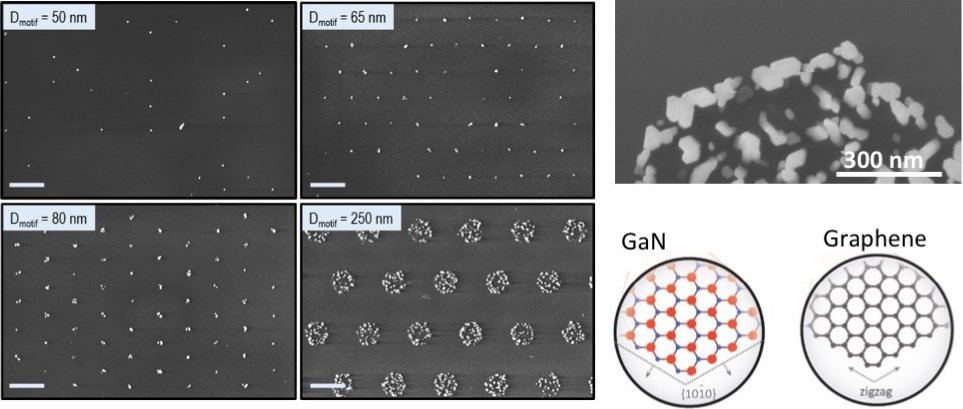
3. Selective area epitaxy of nitride nanowires on graphene nanodots
We demonstrated a new approach to achieve selective area growth of GaN nanowires by plasma-assisted molecular beam epitaxy. The nanowires are grown on graphene nanodots which are patterned by electron beam lithography from polycrystalline graphene patches transferred to SiO2 substrates. The GaN nanowires grow on these graphene domains with a perfect selectivity with respect to the SiO2 surrounding surface. The results demonstrate that a single monolayer of graphene can withstand the lithography process without losing its ability to induce epitaxial growth. The nanowire length distribution and patterns’ fill factor are analyzed in the framework of a theoretical model, which takes into account an incubation time dependent on the graphene dot size. Overall, these results represent the first demonstration of selective area nanowire growth on a regular array of graphene nano-domains.
Van der Waals epitaxy is an attractive method to grow crystalline materials with no strong requirement of lattice matching with the underlying material. The developped novel approach of III-nitride Van der Waals epitaxy on graphene combined with selective area growth opens new prospects for the fabrication of flexible micro-LEDs.
[Man19] Mancini L, Morassi M, Sinito C, Brandt O, Geelhaar L, Song J, Cho YH, Guan N, Cavanna A, Njeim J, Madouri A, Barbier C, Largeau L, Babichev A, Julien FH, Travers L, Oehler F, Gogneau N, Harmand JC, Tchernycheva M « Optical properties of GaN Nanowires grown on chemical vapor deposited-Graphene.” Nanotechnology 30 214005 (2019) doi: 10.1088/1361-6528/ab0570.
[Mor20] Morassi, M; Guan, N; Dubrovskii, VG; Berdnikov, Y; Barbier, C; Mancini, L; Largeau, L; Babichev, AV; Kumaresan, V; Julien, FH ; Travers, L; Gogneau, N; Harmand, JC; Tchernycheva, M ; “Selective Area Growth of GaN Nanowires on Graphene Nanodots” CRYSTAL GROWTH & DESIGN, Volume: 20 ( 2) 552-559 (2020) DOI: 10.1021/acs.cgd.9b00556
[Bar20] Barbier, C; Zhou, T; Renaud, G; Geaymond, O; Le Fevre, P; Glas, F; Madouri, A ; Cavanna, A ; Travers, L; Morassi, M; Gogneau, N; Tchernycheva, M; Harmand, JC; Largeau, L “In Situ X-ray Diffraction Study of GaN Nucleation on Transferred Graphene” CRYSTAL GROWTH & DESIGN Volume: 20 (6) 4013-4019 (2020) DOI: 10.1021/acs.cgd.0c00306
4. Piezoelectric properties of nitride nanowires
Nitride piezoelectric nanowires are promising nanomaterials for high-efficiency piezoelectric generators.
A systematic multi-scale analysis, going from single wire properties to macroscopic device fabrication and characterization, allowed to establish for GaN nanowires the relationship between the material properties and the piezo-generation and to propose an efficient piezo-generator design. The piezo-conversion of individual MBE-grown p-doped GaN nanowires in a dense array is assessed by atomic force microscopy equipped with Resiscope module yielding an average output voltage of 228 ± 120 mV and a maximum value of 350 mV generated per nanowire. In the case of p-doped GaN nanowires, the piezo-generation is achieved when a positive piezo-potential is created inside the nanostructures, i.e. when the nanowires are submitted to a compressive deformation. Moreover, we established the relationship between their mechanical characteristics and their piezoelectric conversion properties using an upgraded AFM technique. This upgraded AFM tool allows probing the piezo-conversion properties of GaN NWs under axial compression with a well-controlled applied force. With this controlled mechanical input, we quantified the mechanical characteristics of the tested 1D-nanostructures and established the direct correlation between the mechanical properties of the GaN NWs and their output voltage generated in response of their axial deformation. We also demonstrated that the insertion of InGaN heterostructures enhances the piezoresponse.
The understanding of the piezo-generation mechanism in our GaN nanowires gained from AFM analyses is applied to design a piezo-generator operated under compressive strain. Nitride nanowires were embedded into dielectric membranes and their mechanical properties were assessed. Piezoelectric generation was investigated both on the level of individual nanowires and on the macroscopic device level. In particular, we have demonstrated the piezo-generator integrating a vertical array of GaN nanowires. The device consisted of nanowire arrays of several square millimeters in size embedded into spin-on glass with a Schottky contact for rectification and collection of piezo-generated carriers. The generator delivers a maximum power density of ∼12.7 mW/cm3. This value settled the new state of the art for piezo-generators based on GaN nanowires and more generally on nitride nanowires, and offers promising prospects for the use of GaN nanowires for high-efficiency ultra-compact energy harvesters.

[Gog16] N Gogneau, N Jamond, P Chrétien, F Houzé, E Lefeuvre, M Tchernycheva « From single III-nitride nanowires to piezoelectric generators: New route for powering nomad electronics », Semiconductor Science and Technology 31 (10), 103002 (2016).
[Jam16] Nicolas Jamond, Pascal Chrétien, Frédéric Houzé, L Lu, L Largeau, O Maugain, Laurent Travers, Jean-Christophe Harmand, Frank Glas, E Lefeuvre, M Tchernycheva, N Gogneau, « Piezo-generator integrating a vertical array of GaN nanowires », Nanotechnology 27 (32), 325403 (2016)
[Lu18] L Lu, E Charron, E Glushkov, N Glushkova, B Bonello, F H Julien, N Gogneau, M Tchernycheva, O Boyko « Probing elastic properties of nanowire-based structures », Applied Physics Letters, Volume 113, Issue 16, Page 161903 (2018).
[Mor18] Martina Morassi, Ludovic Largeau, Fabrice Oehler, Hyun-Gyu Song, Laurent Travers, Francois H Julien, Jean-Christophe Harmand, Yong-Hoon Cho, Frank Glas, Maria Tchernycheva, Noelle Gogneau “Morphology Tailoring and Growth Mechanism of Indium-Rich InGaN/GaN Axial Nanowire Heterostructures by Plasma-Assisted Molecular Beam Epitaxy”, Crystal Growth & Design Volume 18, Issue 4, Pages 2545-2554 (2018).
[Jeg18] Nikoletta Jegenyes, Martina Morassi, Pascal Chrétien, Laurent Travers, Lu Lu, Francois H Julien, Maria Tchernycheva, Frédéric Houzé, Noelle Gogneau «High Piezoelectric Conversion Properties of Axial InGaN/GaN Nanowires », Nanomaterials Volume 8, Issue 6, Page 367 (2018).
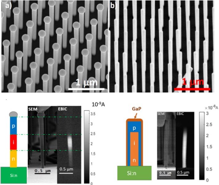
5. Nanoscale photovoltaic properties of GaAsP nanowires for flexible solar cells
For nanowire solar cells standard macroscopic photovoltaic characterization averaged over millions of nano-objects does not provide all the information necessary to understand the device physics and to optimize the performance. It is essential to push the comprehensive analyses down to the nanometric scale and to probe individual nanowire p-n junctions in order to analyze the material quality, to assess the wire-to-wire homogeneity and to detect eventual failures.
Axial p-n and p-i-n junctions in GaAs0.7P0.3 nanowires are demonstrated and analysed using electron beam induced current microscopy. Organized self-catalysed nanowire arrays are grown by molecular beam epitaxy on nanopatterned Si substrates. The nanowires are doped using Be and Si impurities to obtain p- and n-type conductivity, respectively. A method to determine the doping type by analysing the induced current in the vicinity of a Schottky contact is proposed. It is demonstrated that for the applied growth conditions using Ga as a catalyst, Si doping induces an n-type conductivity contrary to the GaAs self-catalysed nanowire case, where Si was reported to yield a p-type doping. Active axial nanowire p-n junctions having a homogeneous composition along the axis are synthesized and the carrier concentration and minority carrier diffusion lengths are measured.
Next, the nanowires were in-situ passivated with a GaP shell. Comparison between non-passivated and passivated nanowires shows a strong enhancement of the collection region after passivation. The results also prove the existence of a p-doped shell around the nanowires formed due to a parasitic radial growth. This shell is depleted in non-passivated nanowires, however it becomes electrically active after surface passivation modifying the carrier collection pattern.
Finally, nanowire array devices were fabricated by encapsulating the nanowires in a transparent polymer and contacting them with indium tin oxide electrode. Electron beam induced current microscopy in top view configuration is used to probe the current generated by individual nanowires within this macroscopic device as well as to analyse the homogeneity of the signal.
[Sak20a] O. Saket, C. Himwas, A. Cattoni, F. Oehler, F. Bayle, S. Collin, L. Travers, A. Babichev, F. H. Julien, J. C. Harmand, and M. Tchernycheva, « Influence of surface passivation on the electrical properties of p–i–n GaAsP nanowires” Appl. Phys. Lett. 117, 123104 (2020); doi 10.1063/5.0022157
[Sak20b] Saket, O ; Himwas, C ; Piazza, V ; Bayle, F; Cattoni, A; Oehler, F; Patriarche, G; Travers, L; Collin, S; Julien, FH; Harmand, JC; Tchernycheva, M; “Nanoscale electrical analyses of axial-junction GaAsP nanowires for solar cell applications” NANOTECHNOLOGY 31 (14) 145708 (2020) DOI: 10.1088/1361-6528/ab62c9
[Sak19] Omar Saket, Chalermchai Himwas, Andrea Cattoni, Fabrice Oehler, Stephane Collin, Francois H Julien, Jean-Christophe Harmand, Maria TchernychevaProceedings “Nanoscale Electrical Characterization of Organized GaAsP Nanowires for Photovoltaic Energy Harvesting” IEEE of 14th Nanotechnology Materials and Devices Conference (NMDC), reference number 19629682 (2019) DOI: 10.1109/NMDC47361.2019.9084020
[Him19] Charlermchai Himwas, Stéphane Collin, Hung-Ling Chen, Gilles Patriarche, Fabrice Oehler, L Travers, O Saket, F H Julien, J-C Harmand and M Tchernychevaet “Correlated optical and structural analyses of individual GaAsP/GaP core–shell nanowires”. Nanotechnology, 2019, 30 (30), pp. 304001. doi 10.1088/1361-6528/ab1760
[Him17] C Himwas, S Collin, P Rale, N Chauvin, G Patriarche, F Oehler, F H Julien, L Travers, J-C Harmand and M Tchernycheva, „In situ passivation of GaAsP nanowires” Nanotechnology 28 495707 (2017).
